- Wafer/ Substrate Parameter : Up to 4 Inch Substrate and Small Wafer pieces can be handled
- Mask Parameter : Can handle up to 5 Inch ( 4 Inch Area Exposable).
- Alignment Accuracy : 0.5µm for Top Side (with 20x). 1µm for Bottom Side (with 20x).
- Separation/ Proximity Adjustment : A maximum of 300µm adjustable in 1µm steps
- Contact Force between Mask and Substrate : Adjustable from 0.5N – 40N.
- Contact Modes : Soft, Hard, Vacuum, Vacuum + Hard, Proximity
- Printing Resolution : 3µm in Proximity, 1µm in Vacuum + Hard Contact
- Lamp House : Standard NUV of 365nm and Standard Lamp Power of 500W
ABM Mask Aligner_Annexe1
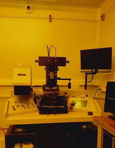
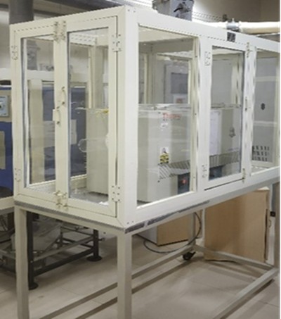
ABM Mask Aligner is a “SEMI-AUTOMATIC” Contact Photo-Lithographic Alignment and Exposure Tool. It also has the Capability of Front to Back Alignment of Patterns and Aligning wafer stack for the Anodic bonder. Recipes for different Exposure types and Contact Modes can be Pre-Written and is very User friendly. The equipment for Optical Lithography allows for selectively masking and exposure of certain areas of
the sample substrate using a ”MASK” and ”SET OF MASK”. Masks are realized in advance by Laser Writer by Etching a Thin Metallic Layer deposited onto a special Glass Slide.
Power source – UV LED
Wavelength – 365nm,405nm
Minimum feature – 0.5um
Auto focus – No
Backside Alignment – Optical light
Contact modes – Soft, Proximity
Auto WEC correction – Yes
Mask sizes – 3″,4″ and 5″
Wafer size – 1″ to 4″
This section will be updated soon.
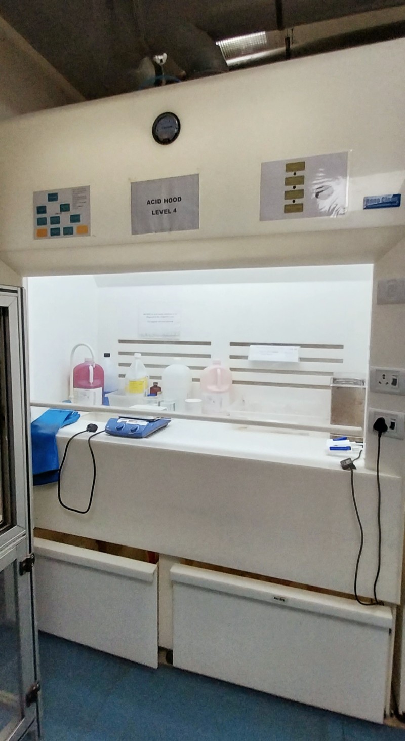
Acid Hood (Annexe 2)
Chemical Wet bench Acids is used for Piranha Cleaning/ HF dip/ Metal/Metal oxide etching of LEVEL 4 samples coming from lithography or other level 4 equipment’s (PV Lab Samples).
Process Capability
Piranha, RCA, Etching
Tool Capability
It has dedicated petridishes and Magnetic stirrer with heater. The bench is also fitted N2 dryer.
This section will be updated soon.
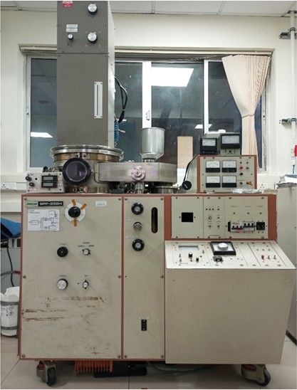
Anelva RF Sputtering – Annexe-1
RF Sputtering runs an energetic wave through an inert gas in a vacuum chamber which becomes ionized. The target material or cathode of the desired material is bombarded by these high energy ions sputtering off atoms as a fine spray covering the substrate to be coated. RF Magnetron sputtering uses magnets behind the negative cathode to trap electrons over the negatively charged target material, so they are not free to bombard the substrate, allowing for faster deposition rates.
Substrate type: Si, Glass, Sapphire, Ceramic, Metal, etc.
Sample Size: From 2mm cut pieces to 2-inch full wafer
Power supply: RF power (3 different magnetrons)
Gases available: Ar
Substrate heating: No
Pumping Combination: Rotary + Diffusion pump
This section will be updated soon.
Anelva RIE System-Annexe-1
Anelva RIE DEM-451 parallel plate, 13.56 MHz system used for etching with tetrafluoromethane (CF4). This system etches substrates placed on the cathode by accelerating active (highly reactive gas) ions dissociated in discharged plasma in the electric potential drop region. The system is used primarily for etching Si, SiO2 and polymide films.
Capabilities: 14″ cathode for large sample sizes or multiple samples.
Power: RF power – 500 W
Electrode Voltage: 200 V to 1 kV
Current: 500 mA
Gas lines: Ar, N2, O2 (100 sccm), CF4 (50 sccm)
Vacuum: Base pressure 10-6 mbar.
Water line temperature: 15 °C to 25 °C
Chamber baking: 200 °C
This section will be updated soon.
Chemical Mechanical Polishing (CMP -Annexe-1)
Chemical-mechanical polishing (CMP) is often associated with chemical-mechanical planarization which is a polishing process assisted by chemical reactions to remove surface materials. CMP is a standard manufacturing process practiced at the semiconductor industry to fabricate integrated circuits. When the purpose is to remove surface materials, it is referred to as chemical-mechanical polishing. However, when the purpose is to flatten a surface, it is referred to as chemical mechanical planarization. CMP is a tribochemical process because of the synergy between friction and corrosion.
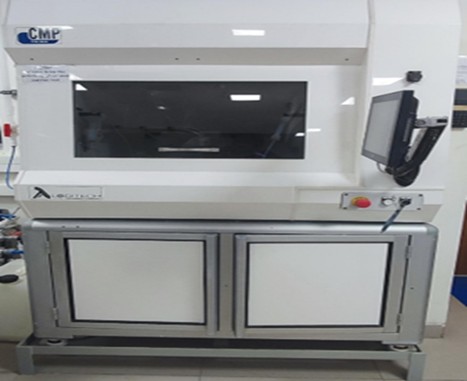
Si Substrate only
Sample Size: 1inch to 4inch wafers
Materials polishing available: Si, SiO2 and SiN
Minimum and Maximum thickness available: 50nm and 1µm
This section will be updated soon.
E-Beam Evaporator_Annex
Electron-beam evaporation, uses a focused beam of electrons to heat the metal for deposition. A controlled deposition of thin-films is achieved. Both dielectrics and metals can be deposited using solid sources.
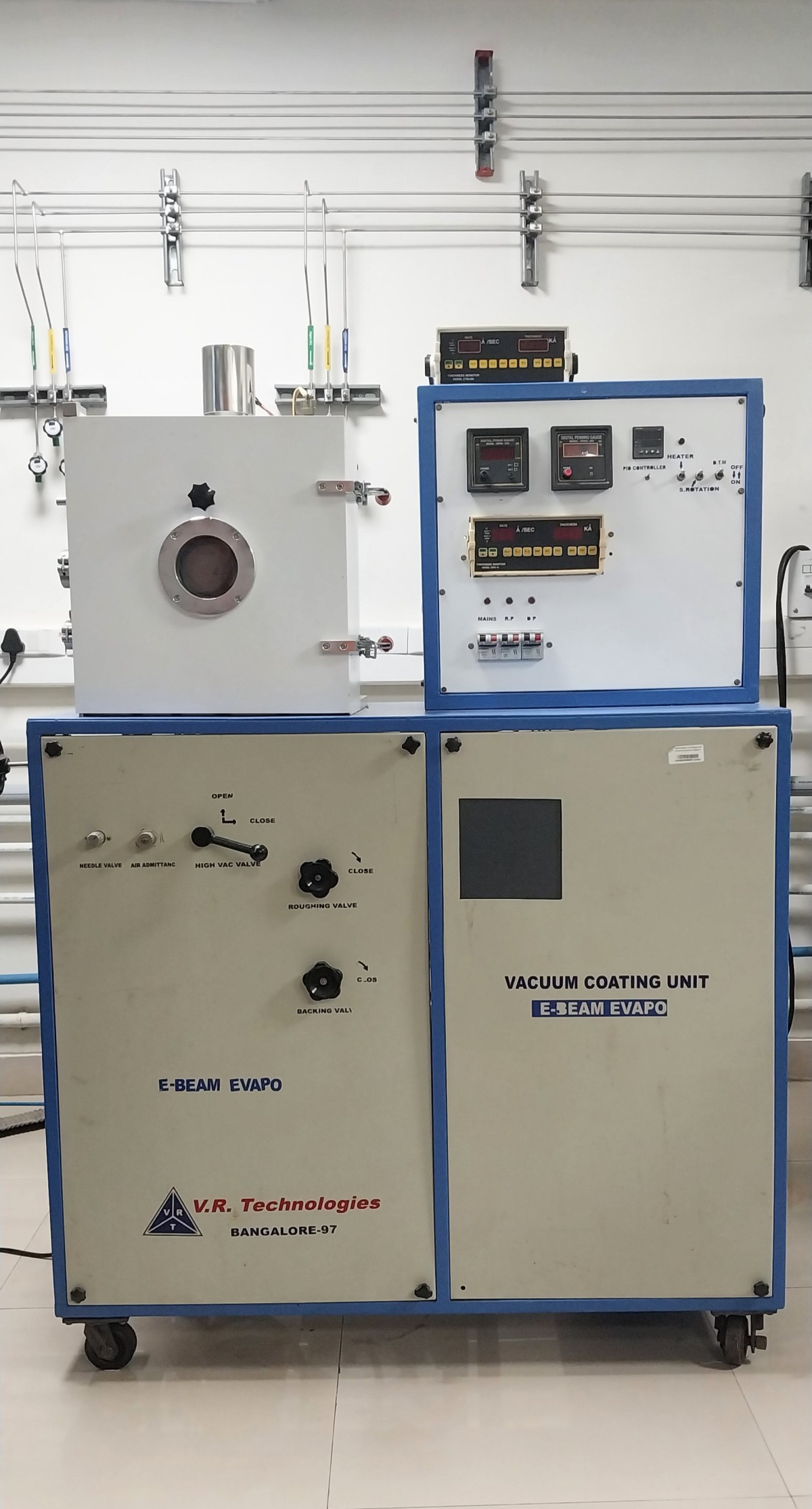
Thickness: 10nm to 150nm Materials available: Cr, Ti, Ag, Au, Ni, & ITO, Al2O3
Substrate holder: One holder with 4-inch area
This section will be updated soon.
HHV Co-Sputter Oxide Tool _Annexe 3
Sputter deposition is a widely used technique to deposit thin films on substrates. The technique is based upon ion bombardment of a source material, Ion bombardment results in a vapour due to a purely physical process; sputter deposition is the use of a magnetron source in which positive ions present in the plasma of a magnetically enhanced glow discharge bombard the target. The target can be powered in different
ways, ranging from dc for conductive targets, to RF for nonconductive targets, to a variety of different ways of applying current and/or voltage pulses to the target.
Substrate Uniformity: 2″
Substrate temperature: 650 C
Power Supplies: RF/DC/PDC
Cathodes: 2
Gas: Ar,O2, N2
Substrate rotation: No
Thickness: 5 nm to 1µm
RGA monitoring available
This section will be updated soon.
HHV Glove Box Sputtering_Annex
Sputter deposition is a widely used technique to deposit thin films on substrates. The technique is based upon ion bombardment of a source material, Ion bombardment results in a vapour due to a purely physical process; sputter deposition is the use of a magnetron source in which positive ions present in the plasma of a magnetically enhanced glow discharge bombard the target. The target can be powered in different ways, ranging from dc for conductive targets, to RF for nonconductive targets, to a variety of different ways of applying current and/or voltage pulses to the target.
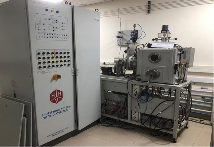
Substrate Uniformity: 3″
Substrate temperature: Nil
Power Supplies: RF/DC/PDC
Cathodes: 3
Power: DC and RF
Gas: Ar,O2
Substrate rotation: 30 rpm
Thickness: 5 nm to 500 nm
This section will be updated soon.
HHV Sputter Coater 2- Annexe 1
Sputter deposition is a widely used technique to deposit thin films on substrates. The technique is based upon ion bombardment of a source material, Ion bombardment results in a vapour due to a purely physical process; sputter deposition is the use of a magnetron source in which positive ions present in the plasma of a magnetically enhanced glow discharge bombard the target. The target can be powered in different
ways, ranging from dc for conductive targets, to RF for nonconductive targets, to a variety of different ways of applying current and/or voltage pulses to the target.
Materials: Ti, Pt, PZT
Cathodes: 3
Power: DC and RF
Gas: Ar,O2
Substrate size: 5” (4”sample can accommodate)
Substrate temperature: 600°C
Substrate rotation: 20 rpm
Thickness: 5 nm to 200 nm
This section will be updated soon.
HHV Sputter Metal Coater1- Annexe 1
Sputter deposition is a widely used technique to deposit thin films on substrates. The technique is based upon ion bombardment of a source material, Ion bombardment results in a vapour due to a purely physical process; sputter deposition is the use of a magnetron source in which positive ions present in the plasma of a magnetically enhanced glow discharge bombard the target. The target can be powered in different ways, ranging from dc for conductive targets, to RF for nonconductive targets, to a variety of different ways of applying current and/or voltage pulses to the target.
Materials available: Au, Ti, Cr, Pt, Ag, Pd, Al
O2 , N2 & Ar MFCs available.
Substrate heater capacity: 400⁰C.
Uniformity: 4” dia.
Power Supplies: DC/RF
This section will be updated soon.
HHV Sputter Tool (Nitride)_Annexe 3
Sputter deposition is a widely used technique to deposit thin films on substrates. The technique is based upon ion bombardment of a source material, Ion bombardment results in a vapour due to a purely physical process; sputter deposition is the use of a magnetron source in which positive ions present in the plasma of a magnetically enhanced glow discharge bombard the target. The target can be powered in different ways, ranging from dc for conductive targets, to RF for nonconductive targets, to a variety of different ways of applying current and/or voltage pulses to the target.
Substrate Uniformity: 2″
Substrate temperature: 650 C
Power Supplies: RF/DC/PDC
Cathodes: 1
Gas: Ar, N2
Substrate rotation: No
Thickness: 5 nm to 1µm
RGA monitoring available
This section will be updated soon.
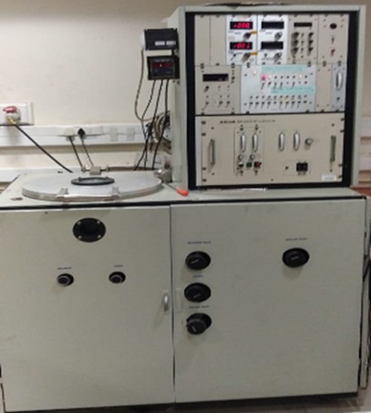
Lindberg Furnace (Annexe-1)
Annealing is a heat treatment procedure involving heating the materials and holding it at a certain temperature (annealing temperature), followed by controlled cooling. Annealing results in relief of internal stresses, softening, chemical homogenizing and transformation of the grain structure into more stable state.These operations are carried out by heating to the required temperature followed by soaking at this temperature for sufficient time to allow the material to stabilize followed by slow cooling (except for solution annealing) at a slow and often times-controlled rate.
Maximum Operating Temperature: 900ºC
Uniform Heating Zone: 22 cms
Gases: Argon, Nitrogen and Oxygen
Samples: 2” substrates
Pressure: Ambient condition
This section will be updated soon.
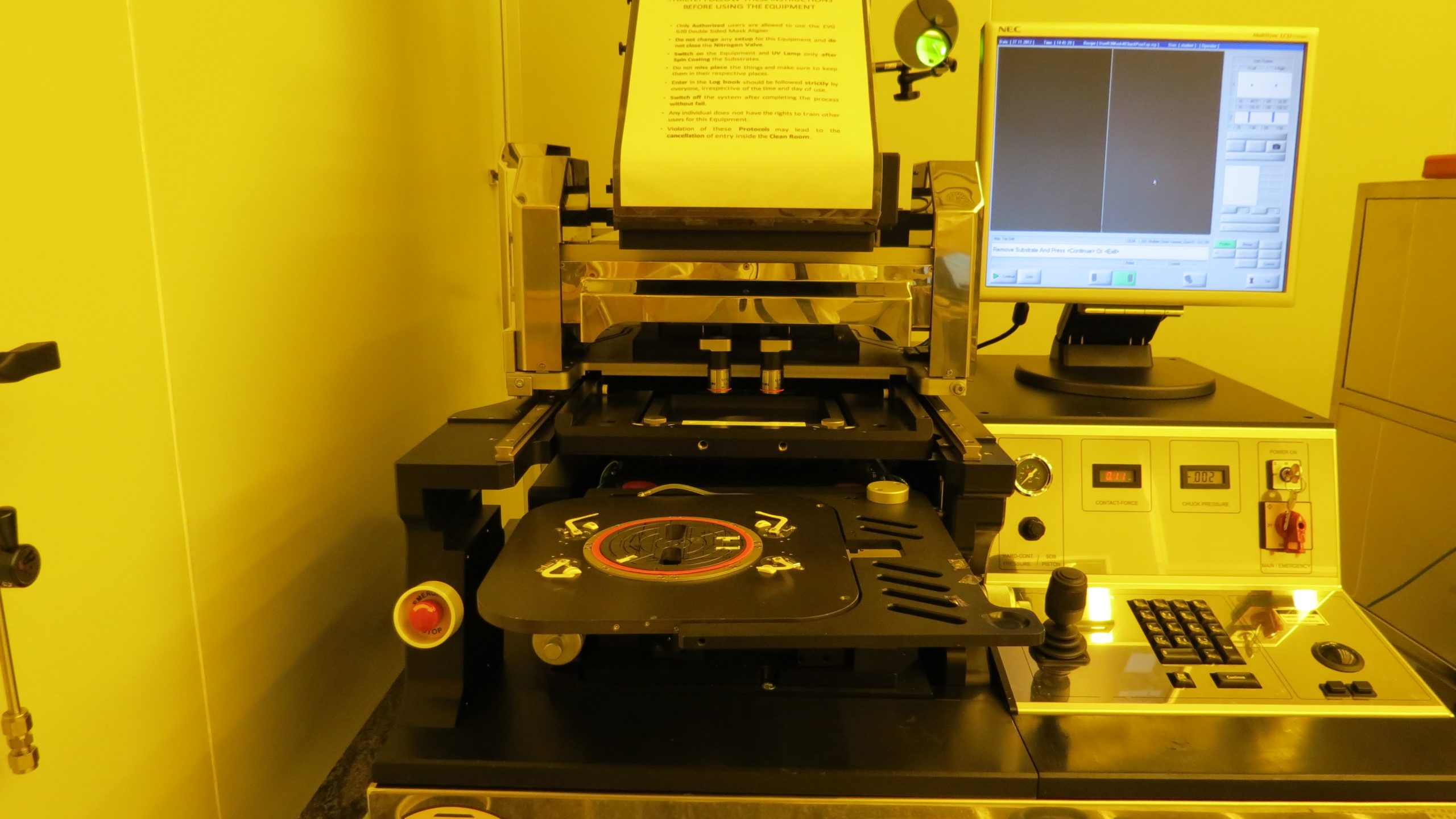
Optical Lithography-EVG 620
EVG620 is a “SEMI-AUTOMATIC” Contact Photo-Lithographic Alignment and Exposure Tool. It also has the Capability of Front to Back Alignment of Patterns and Aligning wafer stack for the Anodic bonder. Recipes for different Exposure types and Contact Modes can be Pre-Written and is very User friendly. The equipment for Optical Lithography allows for selectively masking and exposure of certain areas of the sample substrate using a ”MASK” and ”SET OF MASK”. Masks are realized in advance by Laser Writer by Etching a Thin Metallic Layer deposited onto a special Glass Slide.
This section will be updated soon.
Solvent Hood (Annexe 2)
Chemical Wet bench Solvent/basesis used for solvent clean/ Si etch of samples coming from lithography or other level 4 equipment’s (PV Lab Samples)
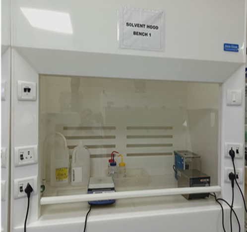
Process Capability
All processes using Acetone, IPA or methanol. This bench is for metal liftoff, Litho mask cleaning and KOH silicon etch (LEVEL 4)
Tool Capability
It has petridishes and ultrasonic bath for lift off process. Heater and beakers are provided for KOH etch of cut pieces. The bench is also fitted N2 dryer.
This section will be updated soon.
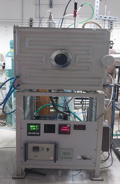
Vacuum Annealing Tool (Annexe1)
Vacuum annealing is a heat treatment process where materials are heated and then slowly cooled under vacuum conditions to relieve stress, alter microstructure, and improve material properties. This process is particularly useful for metals and other materials where surface oxidation or contamination is undesirable, as the vacuum environment prevents reactions with oxygen and other gases.
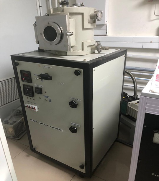
Base pressure : 2 x 10⁻⁶ mbar
Operating pressure: 2 x 10⁻⁶ mbar
Temperature upto : 600°C
Substrate holder size : 6”diameter
Substrate maximum size allowed: 4”
This section will be updated soon.
VR Tech Sputter tool – Annexe-1
Sputter deposition is a widely used technique to deposit thin films on substrates. The technique is based upon ion bombardment of a source material, Ion bombardment results in a vapour due to a purely physical process; sputter deposition is the use of a magnetron source in which positive ions present in the plasma of a magnetically enhanced glow discharge bombard the target. The target can be powered in different ways, ranging from dc for conductive targets, to RF for nonconductive targets, to a variety of different ways of applying current and/or voltage pulses to the target.
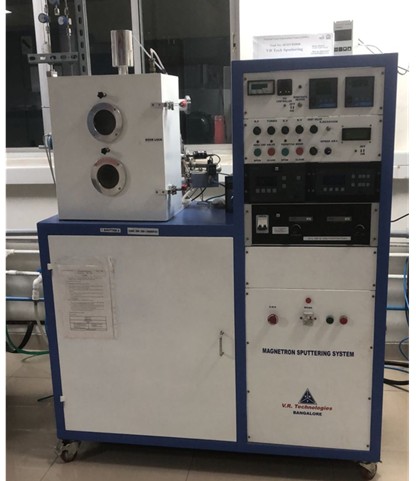
Materials Optimized: Au, Ti, Cr, Pt, Ag, Pd, Al, Cu, Co, NiFe, Ni, Si, Ge, TiW.
Substrate Uniformity 4″
Substrate temperature: Nil
Power Supplies: RF/DC
This section will be updated soon.
VR Tech Thermal Evaporator_Annex
Thermal evaporation is a well-known method for coating a thin layer in which the source material evaporates in a vacuum due to high temperature heating, which facilitates the vapor particles to move directly to the substrate where they condense to solid state.
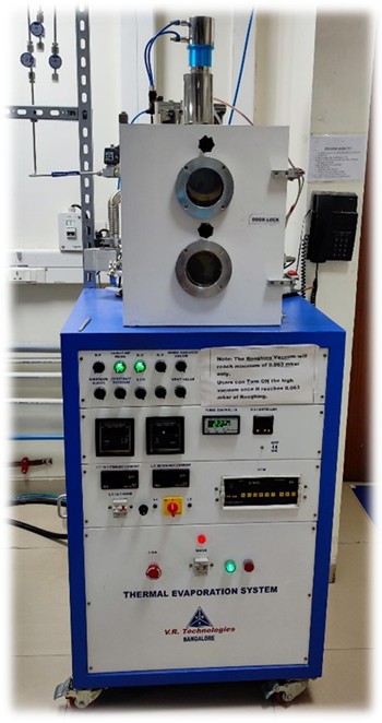
Substrate type: Si, Glass, Sapphire, Ceramic, Metal, etc.
Substrate holder: Up to 4″” dia with substrate rotation and Heating (up to 600°C).
Substrate heating: No
Pumping Combination: Rotary + Turbo
Uses tungsten or molybdenum filaments to evaporate the materials.
Uses Quartz crystal is used to monitor the thickness of the deposited film
This section will be updated soon.