- Profiling surface topography and waviness.
- Measures roughness in the nanometre range.
- The system can produce three-dimensional measurements and analyses when equipped with the 3D Mapping Option.
- Stress measurement of thin film on full inch wafer (2”, 3”, 4”, 6”, and 8”).
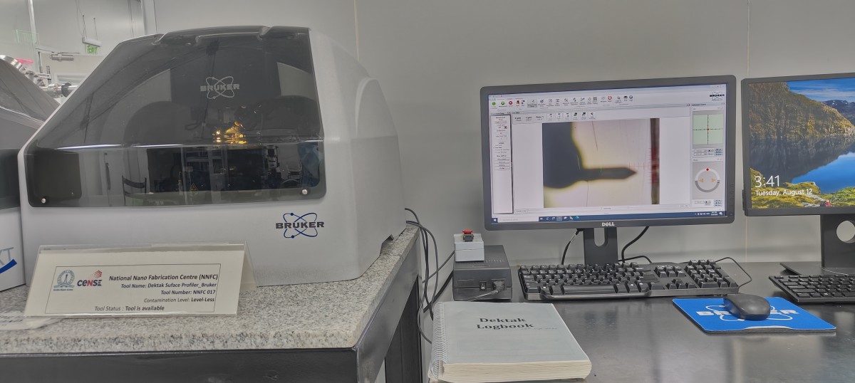
Dektak Suface Profiler_Bruker
The Dektak XT surface profiler is an advanced thin and thick film step height, roughness and 2D stress measurement tool.
This section will be updated soon.
Process Capability
Tool Capability
- Measurement Technique: Stylus Profilometry Contact Measurement
- Measurement Capability: Two Dimensional Surface Profile Measurements
- Stylus Sensor: Low Inertia Sensor
- Stylus Force: 1mg – 15mg LIS 3 Sensor
- Low Force Option: 0.03-1mg
- Stylus Options: 2µ and 12.5µ
- Scan Length: 50mm for 2” and 200mm for 8” with Scan Stitching Capability
- Data Points Per Scan: 120,000 maximum
- Maximum Step Height that can be measured: 800µ
- Minimum Step Height that can be measured: 16nm
This section will be updated soon.
Electro Chemical work station_Annex
The Solartron Analytical Modulab instrument has variety of applications including electrochemical water splitting, photovoltaic IV measurements, and also electrochemical impedance of both solids and solutions. It is an advanced machine for a variety of applications such as super capacitors, fuel cells and batteries.
This section will be updated soon.
Process Capability
Tool Capability
Make: Solatron Analytical
Specifications:
Compliance voltage 8V (without HV module), 30V (with HV30), 100V (with HV100)
Compliance current +/-100mA (without booster module), 2A (with booster module)
Frequencies response analyser module 1MHz
Current resolution 1,5pA (0,15fA with module femto ameter)
Sampling at 1us
This section will be updated soon.
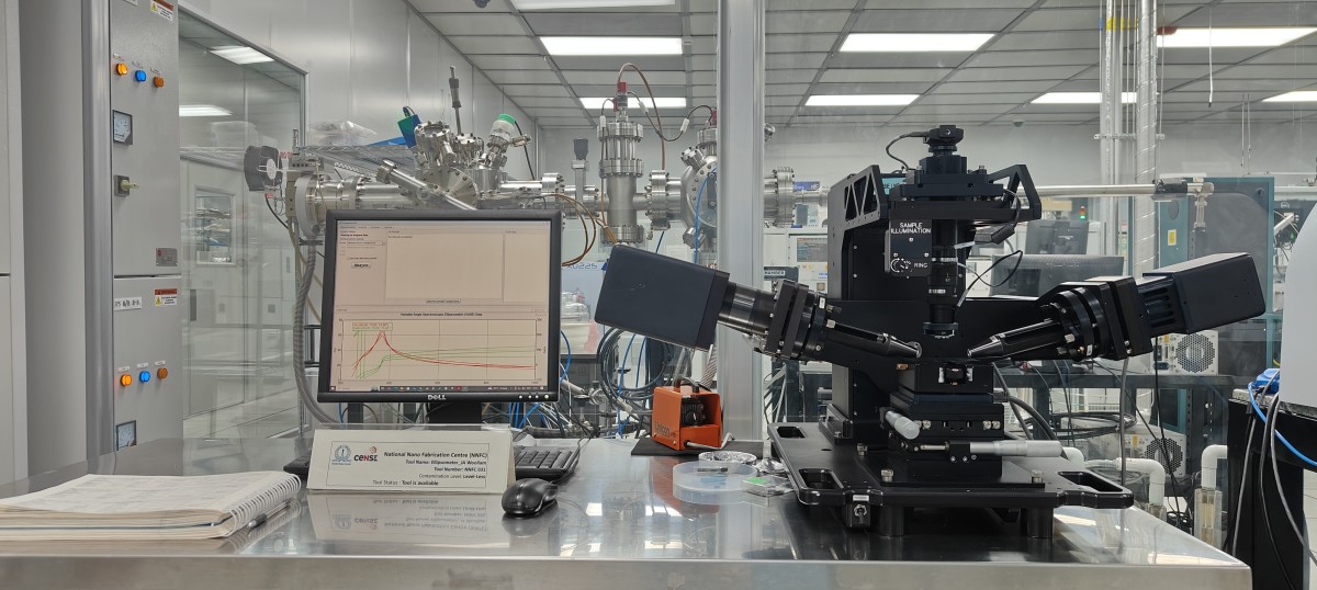
Ellipsometer_JA Woollam
Ellipsometer measures a change in polarization as light reflects or transmits from a material structure. The polarization change is represented as an amplitude ratio, Ψ, and the phase difference, Δ. The measured response depends on optical properties and thickness of individual materials. Thus, Ellipsometer is primarily used to determine film thickness and optical constants. However, it is also applied to characterize composition, crystallinity, roughness, doping concentration, and other material properties associated with a change in optical response.
Process Capability
Standard models available for the following materials
1. SiO2
2. Si3N4 (Low & high stress)
3. PolySi
4. PolyGe
5. LTO
6. a-Si
7. Al2O3
8. TiO2
9. WO3
10. CeO2
11. Gd2O3
12. MgO
13. ITO
14. HfO2
15. ZnO
Tool Capability
Spectral Range: 245-1000nm
Source: Deuterium and Quartz Tungsten Halogen Lamp
Receiver: Single Receiver Unit
Sample Tilt Alignment: Manual
Focusing Option: Available
Camera: High Resolution with 1X-6.5X Variable Zoom Lens
Transparent films up to 10um can be measured.
Measurement of thin film on full 12 inch wafer.
This section will be updated soon.
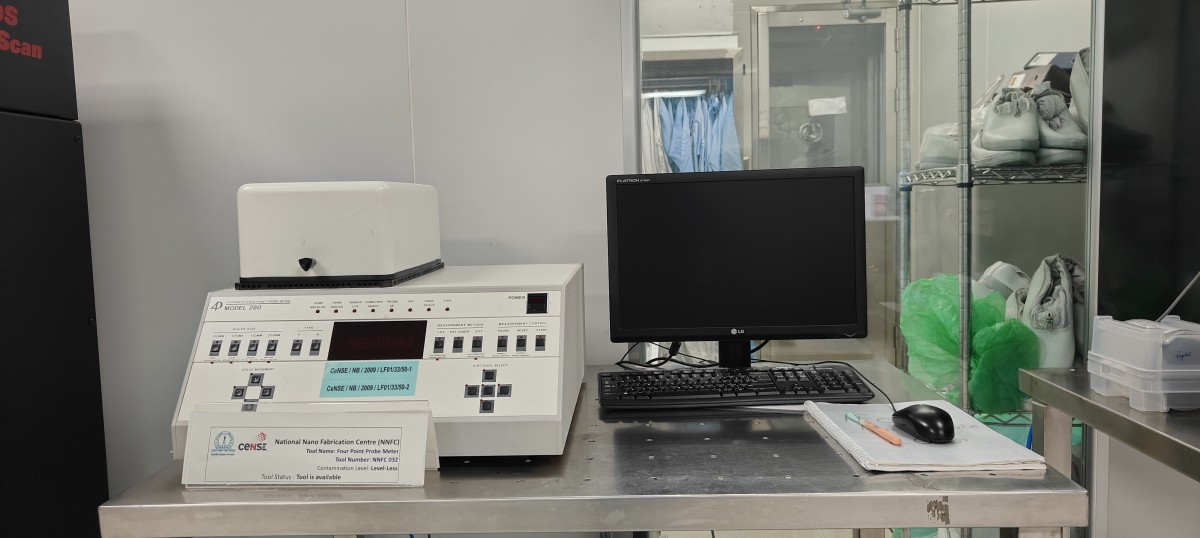
Four Point Probe Meter
A four point probe is a simple apparatus for measuring the resistivity of semiconductor samples. By passing a current through two outer probes and measuring the voltage through the inner probes allows the measurement of the substrate resistivity
Process Capability
Semiconductor and Conductor Materials
Tool Capability
- Wafer or square wafer maximum size: 8-in wafer or 6 x 6 inches square wafers
- Sheet resistance range: from 0.001 Ω/Square to > 800K Ω/Square
- Mapping positions can be close to wafer edge; up to 3mm edge exclusion
- Custom site mapping (number of sites needs to be more than 2)
- Measurement units: Ω/Square, Ohm-cm, V/I, t(μ), t(Å)
- Accuracy of the electronic: < 0.1% (precision resister)
- Measurement repeatability: <0.2% (typ)
- Input impedance: >107 Ohms throughout the measurement range
- Maximum measurement time for a 49-site wafer mapping (test diameter at 194 mm, two configuration method) is less than 1.5 minutes
- Compliance voltage ± 125 Volts in current range from 0.25μA to 250mA
- Current resolution: 16-Bit A/D
- Measurement calibration NIST/VLSI traceable
This section will be updated soon.
IR-VASE Ellipsometer
Ellipsometer measures a change in polarization as light reflects or transmits from a material structure. The polarization change is represented as an amplitude ratio, Ψ, and the phase difference, Δ. The measured response depends on optical properties and thickness of individual materials. Thus, Ellipsometer is primarily used to determine film thickness and optical constants. However, it is also applied to characterize composition, crystallinity, roughness, doping concentration, and other material properties associated with a change in optical response.
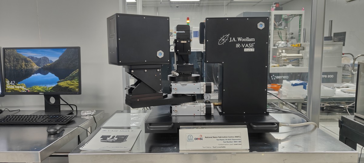
Spectral Range: 1.7-30µm
Resolution from 1cm-1 to 64cm-1
Angel of Incidence 32° to 90°
Source: Silicon Carbide Globar with FTIR Spectrometer
This section will be updated soon.
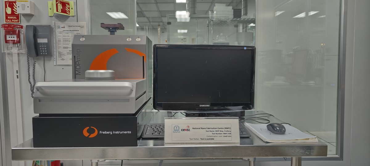
Life Time Measurement_MDP Map_Freiberg
MDPmap is a compact bench top contactless tool for measuring parameters like carrier lifetime, photoconductivity, resistivity and defect information over a wide injection range in steady state or short pulse excitation (μ-PCD). Automated sample recognition and parameter setup allows an easy adaption to a big variety of different samples comprising epitaxial layers and wafers after various preparation stages ranging from as-grown wafers to up to 95% metallized ones
Process Capability
- Mapping Capability of Carrier lifetime & Photoconductivity
Tool Capability
- Sample thickness Range – 10µm to 20mm
- Sample size : 5 x 5 mm2 to 12 inch wafer
- Measurement spot size : 0.5 mm to 10mm
- Excitation Power : 405nm & 980nm laser , Option available to add another external UV laser (355 nm)
- Integrated Heating stage : room temperature to 200°C
- Measurement speed: < 5 minutes for a 6 inch Si wafer, 1 mm resolution
- Range of lifetimes: 20 ns to several ms
This section will be updated soon.
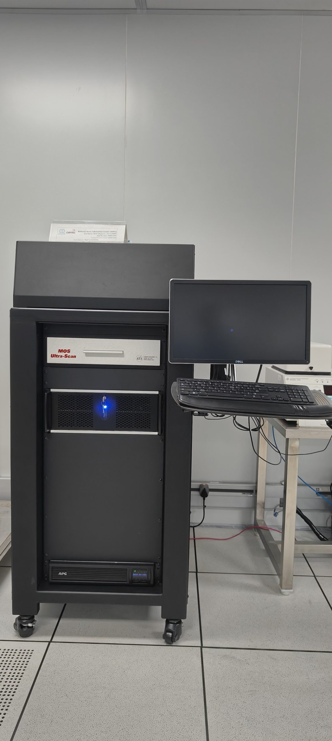
MOS Ultrascan_KSA at NNfC
The Ultra-Scan uses a 2D laser array to map the two-dimensional curvature of semiconductor wafers, optical mirrors, lenses, or practically any polished surface. The system also provides quantitative film stress analysis with full area map scan for wafers by first scanning the bare substrate and then re-scanning the sample post-process.
Process Capability
- Any polished surface with >1% reflectivity at laser λ
- Spatial Scan Resolution: User selectable, down to 1um
Tool Capability
- Scanning is programmable.
- 1cm/1cm sample can be measured.
- Sample size range: 10mmx10mm – 200/300mm diameter
- Bow, Curvature, Tilt etc can be done.
- Various types of scan can be performed(Line, Circular, Rectangle, Custom line/Rectangle)
- Laser Wavelength: 660nm nominal
This section will be updated soon.
Optical Microscope at Inline
Differential interference contrast and high-performance fluorescence capability of the microscope can be used to study various properties of the sample.
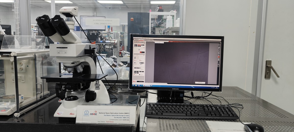
Objectives 5X, 10X, 20X, 50X, 100X, 150X
Oil immersion capability
Binocular
Digital camera (DFC 450C)
Image resolution : 5 megapixels
Bright field, Dark field and fluorescence applications
This section will be updated soon.
Probe Station IV-CV at NNfC
The SourceMeter combines a precise, low-noise, highly stable DC power supply with a low-noise, highly repeatable, high-impedance multimeter. It has 0.012% basic accuracy with 5H-digit resolution.
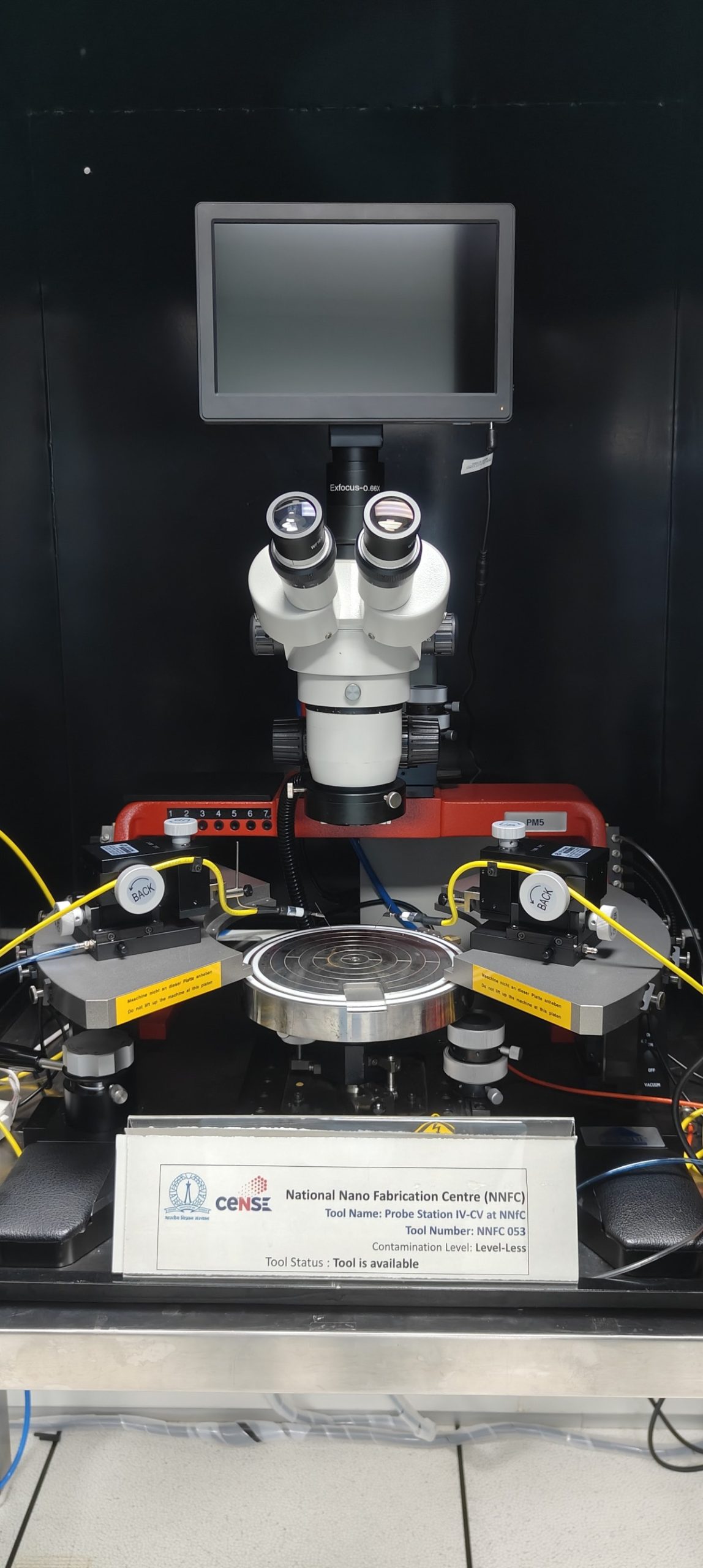
Source voltage — Display current and/or voltage measurement
Source current — Display voltage and/or current measurement
Measure resistance — Display voltage or current component of measurement
Measure only (V or I) — Display voltage or current measurement
This section will be updated soon.
SEM_Phenom XL
Phenom XL G2 is a tabletop SEM equipped with Feild Emission Source of material CeB6. Tool is highly suitable for quick imaging with either Optical or Electron Beam with sample loading time of less than 5 seconds and 60 seconds respectively.

Electron Source – Field Emission Source (CeB6)
Detectors – BSA, SE and EDS
Magnification (Light Optical) – 3 – 19x
Magnification (Electron Optical) – 160 – 200,000x
Digital Zoom – 12x
Resolution – <10nm
Stage Movement – Computer Controlled, Motorized X and Y
Sample Size – Maximum of 100mm x 100mm, Height of 35mm
Image Resolution Options – 690×600, 1920×1200 and 3840 x 2400 pixels
This section will be updated soon.
SEM_Zeiss
Zeiss Gemini 500 is a Schottky field emitter filament equipped Scanning Electron Microscopy. Imaging is possible for sample dimension from 5mm to 100mm diameter wafer.
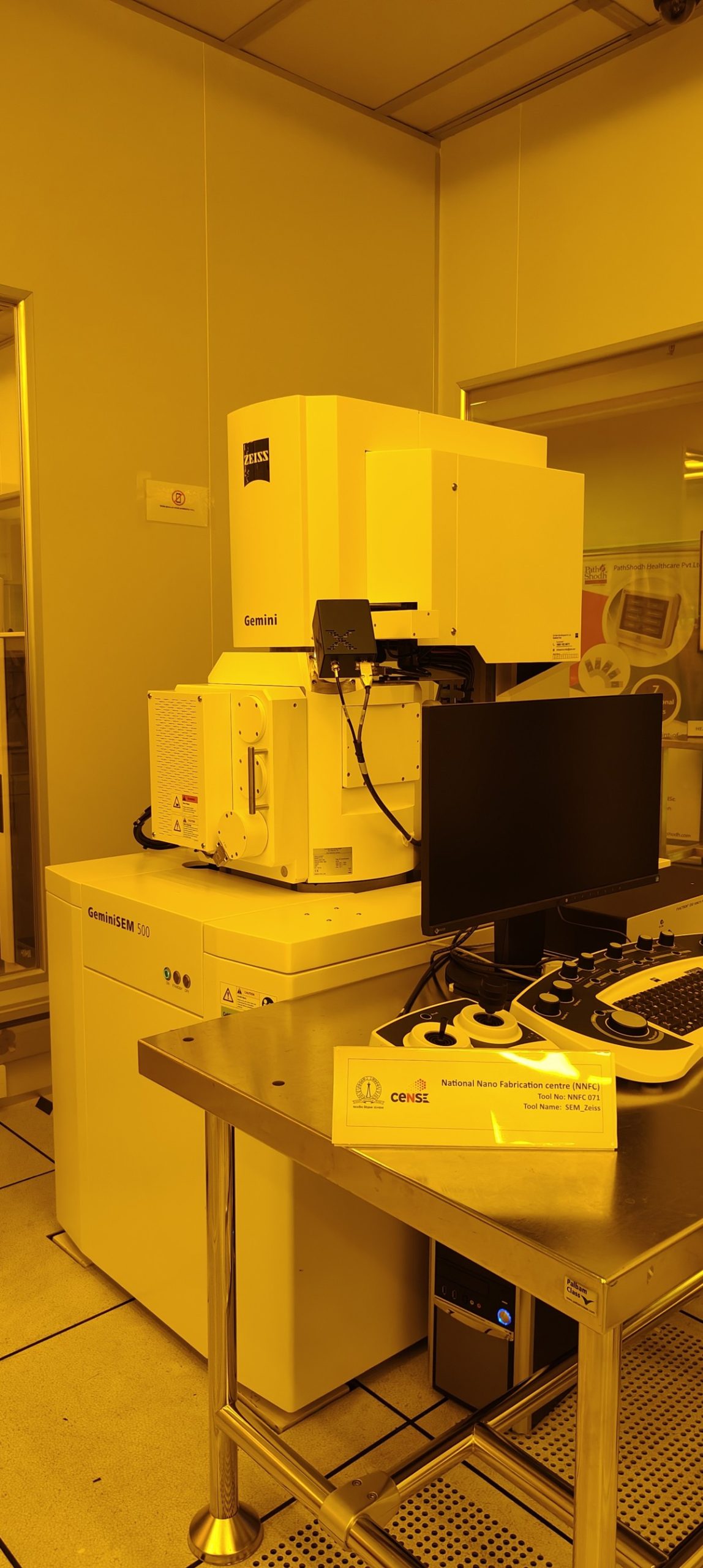
Filament – Schottky field emitter
Acceleration Voltage – 0.02 – 30kV Magnification – 50x – 2,000,000x
Working Distance – 0.1mm – 50mm
Stage Movement – 5-axes motorized eucentric, Controlled by SEM Software as well
as with Dual Joystick Control box
Tilt – -4° to 70°
Apertures – 10µm, 20µm, 30µm, 60µm and 120µm
This section will be updated soon.