RESEARCH

DESCRIPTION
Electrochemical Biosensors
Cost-effective innovations for Healthcare
This group aims at developing electrochemical biosensors for medical diagnostics, with particular attention to Diabetes through cost-effective innovations. Electrochemical Biosensors rely on change in current signal with application of electrode potential. The measurable current signal, obtained due to a redox reaction, depends on the concentration of the biomolecule to be detected. A panel of electrochemical biosensors has already been developed for management of Diabetes and its complications. This includes novel electrochemical sensors for glycated Albumin, glycated Hemoglobin, Microalbminuria, Albumin to Creatinine Ration (ACR). A point-of-care-technology (POCT) based device has been developed on the basis of this research and is being commercialised under a start-up PathShodh Healthcare. Present area of focus is on development of biosensors aimed at early detection of Diabetes and its complications.
Development of Nanosensors and Microfluidics towards
Raman Spectroscopic Applications
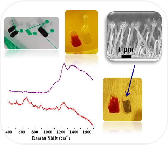
integrated SERS substrates and Centrifugal Microfluidics
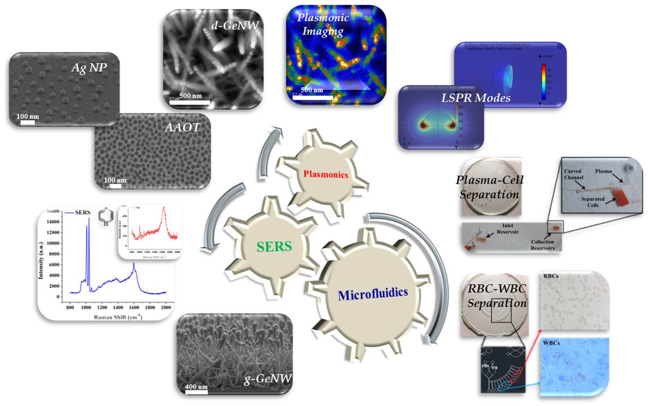
We are interested in investigating the localized surface plasmon resonance (LSPR) modes of metal nanostructures through simulation (COMSOL) and experiment (CL Imaging). Establishing effects of substrate permittivity has enabled us to engineer effective substrates with Ag nanoparticles (AgNP), Anodized Aluminium Oxide Templates (AAOT), AgNP deposited or grown on Germanium Nanowires (d-GeNW, g-GeNW) to name a few.
We are working on centrifugal microfluidics (LOACD) instead of conventional pressure driven microfluidics to avoid the disadvantages related to driving method (usage of expensive syringe pump) and footprint of the setup. We have developed centrifugal microfluidic devices for cell component separation.
We are in a process to integrate both the above mentioned tools and techniques to formulate device/s which can have the capability ranging from laboratory analysis to point-of-care testing. This work has been carried out with our collaborator, Prof. Siva Umapathy at Inorganic and Physical Chemistry Department (IPC).
Gas Sensors Lab
Metal oxide, Flexible and nanostructured sensors for SO2, CO, H2, NO2
Air Quality Monitoring Systems
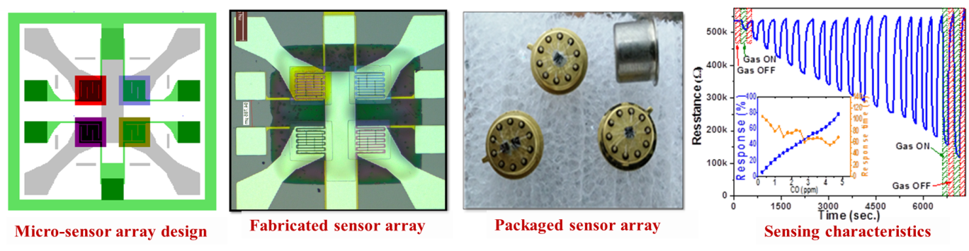
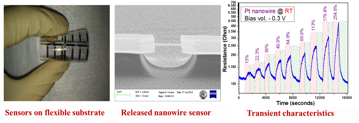
Air pollution affects climate, water, crops, vegetation, animals, wildlife, and adversely impacts personal comfort and well-being. Thus it has become essential to develop reliable and low cost sensors for large scale deployment to monitor air pollutants. In the field of metal-oxide based gas sensors, the major challenges are to reduce the cost of sensors, improve reliability and long term stability with low order of detection, selectivity and low power consumption. Bulk production of nano-sized sensors, sensors on plastic sheets and new sensor device structure are few of the approaches to achieve low effective, low power and high selective sensors. However, the detection precision and response stability of these new architectures still needs more investigation. Currently, we are engaged in developing sensor array platform for portable devices, sensors for flexible electronic and new sensor device architectures for the selective detection of hazardous gases using CMOS compatible process.
Nanostructured Metal Oxide Gas Sensors:
Metal oxide gas sensors are promising for commercial applications. However most of the metal oxide gas sensors suffer from poor selectivity, stability and have high production costs. In order to reduce the cost of the sensors many researchers have focussed on developing gas sensors on low cost substrates like polymers. To improve sensitivity there are efforts to increase the surface to volume ratio by using nanostructures.
We are aiming to tackle the issue faced by conventional metal oxide gas sensors mainly of poor selectivity and high production cost. For improving selectivity we are working on metal oxide heterostructures with surface nanostructuing down to 30nm to enhance sensitivity along with good selectivity.
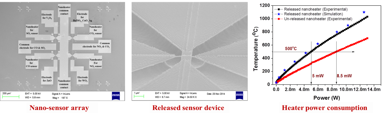
To reduce the cost of the sensors for mass production we are developing sensor array on flexible substrate with CMOS compatible processes. Sensor array consists of individually controlled microheater for four different sensing materials. The materials Vanadium Oxide, Zinc Oxide, Tin Oxide and Tungsten Oxide are used to measure the sensing characteristics for SO2, CO, H2, NO2.
High Electron Mobility Transitors
High Power Electronics
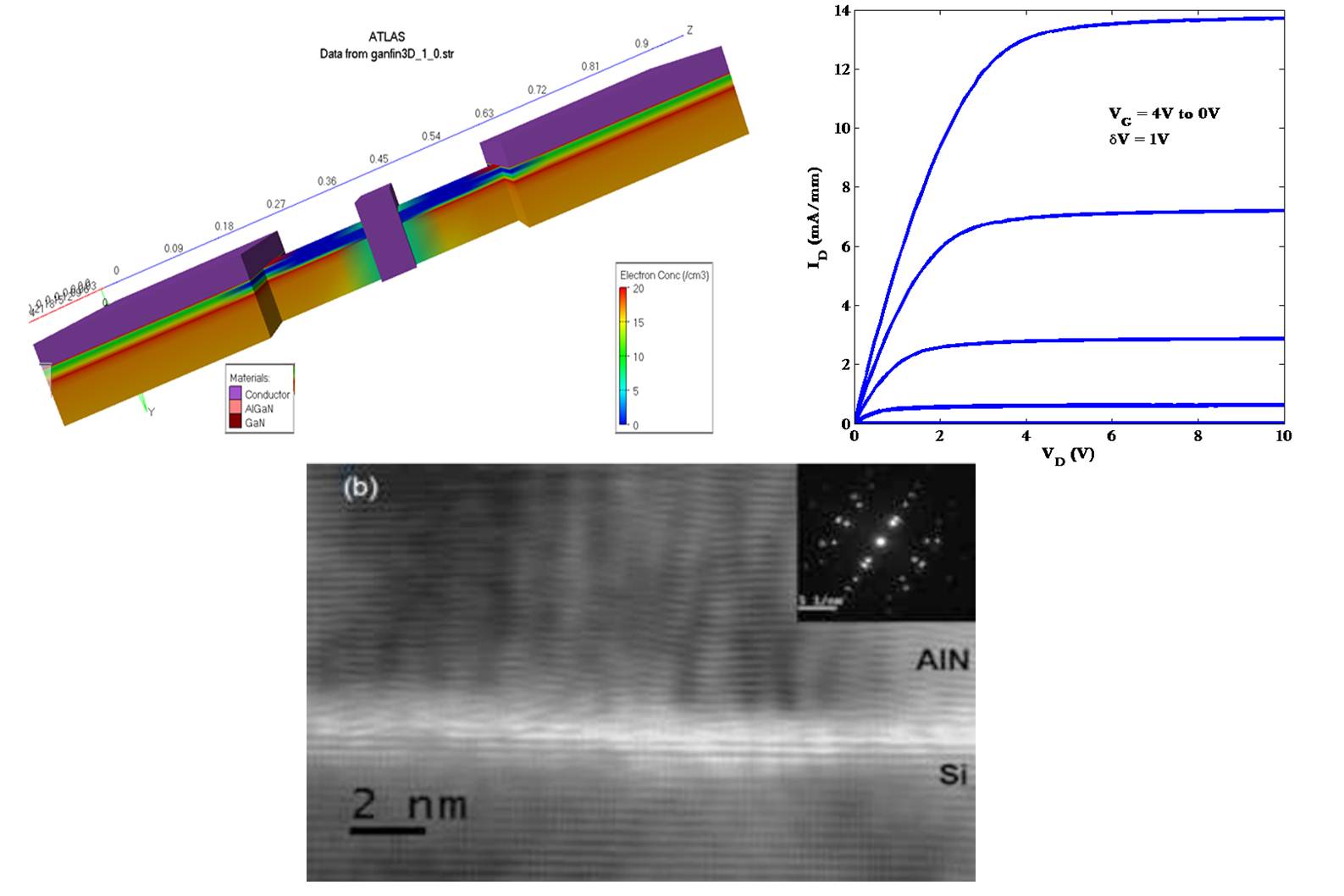
As technology advances, there is growing demand for high-power, high-frequency transistors. To meet it, transistors must be fabricated from a semiconductor with a high breakdown voltage, high mobility and high thermal conductivity. Gallium nitride meets these criteria. As GaN substrates are very expensive, growing GaN layers on an inexpensive substrate like Si is desirable. Because of a large lattice mismatch, it is difficult to grow GaN on Si epitaxially. Thus, the growth process and the growth stack must be designed carefully to obtain crack-free GaN layers on Si. GaN/AlGaN heterojunction high-mobility (HMHT) transistors are being heavily investigated today. However, their normally ON nature poses a significant challenge because the safe operation of power transistors calls for normally OFF behaviour. If this challenge can be met, rapid progress in power electronics may be expected.
Our group works on growth of GaN on Silicon as well as fabrication of normally-off HEMTs. A two dimensional electron gas (2DEG) of mobility above 1500 cm2/Vs and a carrier concentration of 0.8E12 cm-2 has been achieved by proper precleaning of Si wafer and appropriate growth conditions and growth stack. Normally-off HEMTs of threshold voltage above 1V have also been demonstrated with two different approaches namely fluorine ion implantation below gate electrode and gate recess etching technique.
References: Appl. Phys. Lett. 103, 211902 (2016)
2D Nanoelectronics
MoS2 & Graphene
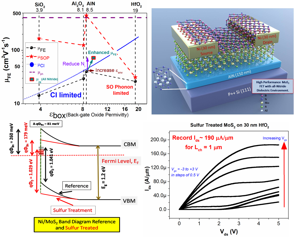
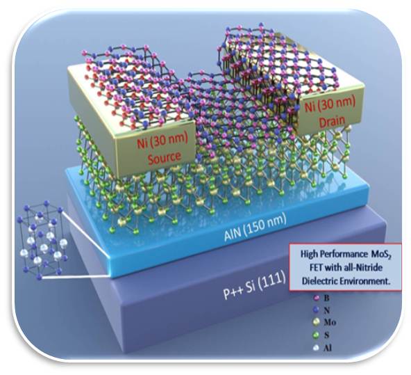
With dimensional scaling encountering fundamental limits with traditional Silicon based MOS FET technology, exploring new materials and device architectures have become crucial to sustain the demands of the semiconductor industry. A new class of Two-dimensional (2D) semiconductors such as Transition Metal Dichalcogenides, which are just one atomic layer thick (or thin!), provides excellent electrostatic control enabling transistor channel lengths in the order of a few nanometers. Using state-of-the art cleanroom and characterisation facilities at CeNSE we aim to solve some of the fundamental roadblocks in realising high performance 2D nanotransistors.
Due to their ultrathin nature, charge transport in 2D semiconductors is heavily influenced by the surrounding dielectric environment. Through experimental data from devices fabricated on several substrates coupled with extensive semi-classical modelling we propose nitride based environments as optimum candidates for gate and encapsulation dielectrics [1]. As a result, high performance transistors with an all nitride dielectric environment are demonstrated on one of the promising 2D semiconductors, Molybdenum disulphide (MoS2). Furthermore, we have solved the large variability and poor contact nature at the metal/MoS2 interface by employing a facile Sulphur Treatment technique [2] yielding record drive currents at 1 micron channel lengths when supplemented with hafnia (HfO2), a CMOS-compatible high-κ gate dielectric [3]. Sulfur Treatment results in substantial reduction of Schottky Barrier Height at the metal/MoS2 interface which provides clear insights into the intrinsic limit of Contact Resistance in multilayer MoS2 FETs [4]. Our current research is focussed towards leveraging on the combined device and materials expertise to develop ultra-low power, highly scaled 2D FETs.
References
[1] S. Bhattacharjee et.al. Adv. Electron. Mater. 1600358(2017)
[2] S. Bhattacharjee et.al. IEEE Trans. Electron Devices 63, 2556–2562 (2016)
[3] K.L. Ganapathi et.al. IEEE Electron Device Letters, 37(6), 797-800 (2016)
[4] S. Bhattacharjee et al. IEEE Electron Device Letters 37.1 (2016): 119-122
Students: Sooraj Sanjay
Nanoelectronics for ISFETs and BioFETs
2D Materials
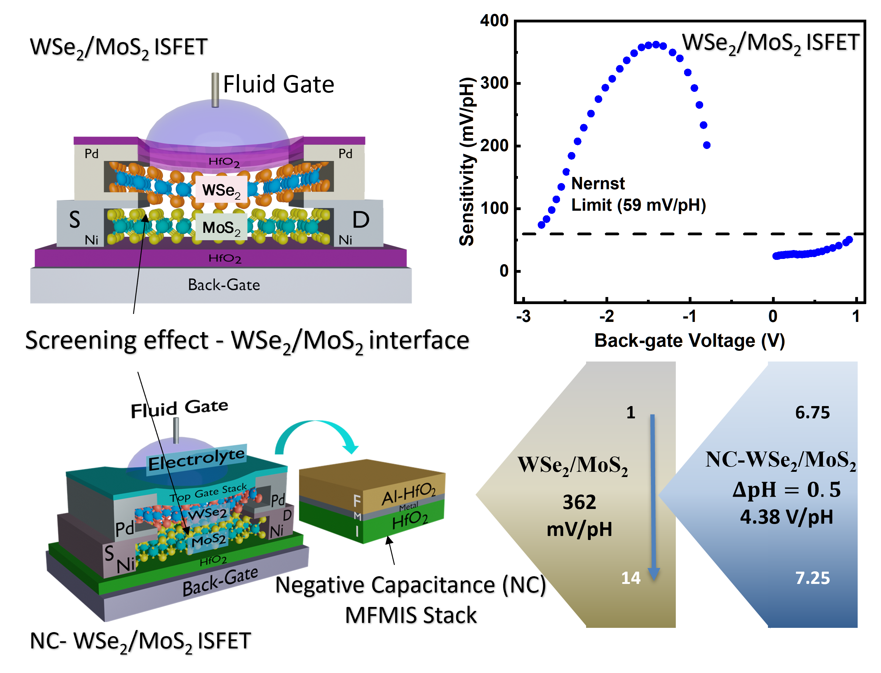
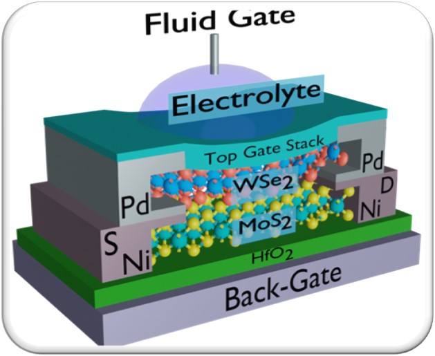
Two-dimensional (2-D) materials show promise for highly scaled nodes because of their atomically thin composition and exceptional electrostatic properties. The remarkable surface-to-volume ratio and sensitivity to external factors also make 2-D materials ideal for bio-sensing applications. By appropriately functionalizing field-effect transistor (FET) technology, ion-sensitive FETs (ISFETs) can be created for detection of pH and various biomolecules.
Despite the advantages of a CMOS platforms, ISFETs suffer from major bottlenecks, which includes limited sensitivity ( < 59 mV/pH, the Nernst limit), need for isolation, and challenges in reliability due to problems like drift. In our lab, we investigate device architectures and innovations to surpass these challenges. The Nernst limit must be surpassed to achieve higher resolution measurements of pH and biomolecules. Through a heterostructure of WSe2 and MoS2, we have demonstrated super-Nernstian pH sensitivity, reaching 346 mV/pH[1]. This device capitalizes on the charge screening effect of the interface and inversion charges at the heterointerface for enhanced sensitivity. Additionally, we've utilized a TCAD-based approach, integrating ferroelectric negative capacitance effect onto the WSe2/MoS2 heterostructure device, and demonstrated sensitivities reaching 4.38 V/pH[2].
Our ongoing research focuses on leveraging these architectures and platforms for biomolecule sensing while concurrently enhancing their stability and repeatability using extended gate devices. We maintain a focus on miniaturizing these devices by utilizing the state of the art nanofabrication facilities at NNFC, CeNSE; thereby enabling them for next generation point-of-care diagnostic devices.
References
[1] S. Sanjay et.al., npj 2D Mater Appl, 5, 93 (2021).
[2] S. Sanjay et.al., IEEE Sensors Journal, 23(12), 12526-12535 (2023).
Students: Sooraj Sanjay, Ananya Tiwari