
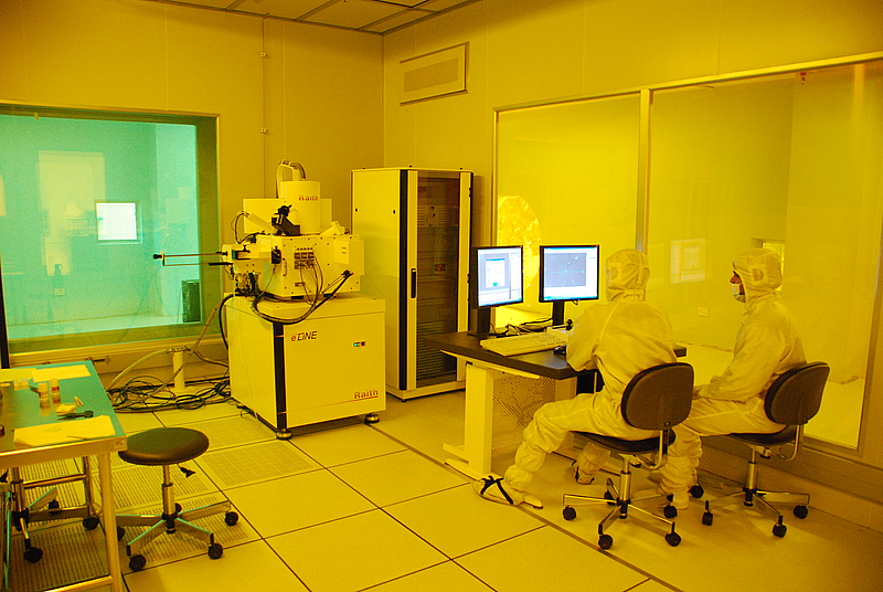
 The National Nanofabrication Centre (NNfC) at the Centre for Nano Science and Engineering (CeNSE) is a CMOS/MEMS/NEMS- capable research facility located at the Indian Institute of Science, Bengaluru (India). This Centre houses state-of-the-art research equipment for both fabrication and in-line characterization of the devices.
The Nanofab is capable of routinely processing 100 mm (4-inch) silicon wafers with a handful of tools that can process larger, 150 mm (6-inch) substrates.
The NNfC has a dedicated staff of nearly 50 engineers and technicians who maintain the process tools and develop unit process modules to support complex process integration for research and prototyping. At CeNSE, we also have access to test and packaging laboratories that can be utilized to characterize and calibrate devices such as MEMS-based RF switches, pressure sensors, gyroscopes, gas sensors and micro-fluidic devices, to name a few. The NNfC has now been fully operational for almost three years, having opened its doors in January 2012.
We have developed several unit processes that involve most of the standard semiconductor operations, starting with optical and eBeam lithography, thin film deposition (ALD, CVD, LPCVD, PECVD), dry etching (RIE, DRIE), thermal processing (oxidation, diffusion), electro-deposition and finally, bonding/dicing & packaging.
We are now taking our research efforts at NNfC to the next level by engaging in process integration of more complex process steps that will involve several lithography mask levels and final device or module prototyping. The panel below illustrates our process integration capability for the fabrication of a microwave cavity device. At our Centre, we have also fabricated novel silicon-carbide cantilever structures, electromechanical acoustic and RF MEMS devices, micro- and nano-machined structures, a full range of pressure sensors (0-400 bar), and even biomedical devices such as micro-needles for insulin delivery. Also seen below is an example of electro-mechanical characterization of a RF MEMS switch using the Laser Doppler Vibrometry technique available at CeNSE. The NNfC staff and scientists also have expertise in building equipment to address non-standard unit modules that are needed in a research facility such as ours. Shown below is one such instrument built by our Centre for scaling up electro-deposition of gold and copper for four-inch wafers. In addition, there are multiple research efforts in silicon-photonics, Neuroelectronics, Photovoltaics, Microfluidics and Compound semiconductor-based devices for both commercial and strategic applications.
Facilities at NNfC may be used by any researcher either from academia or from industry within India and abroad. They are fully computerized, with the capability for online reservation of equipment.