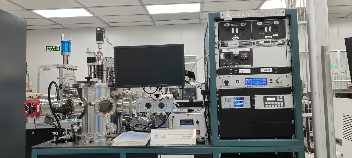
Deposition

Sputter Coater 1 Metals

Sputtering is one of the most widely used techniques for depositing thin films. The target is a plate of the materials to be deposited or the material from which a film is synthesized. Because it is connected to the negative terminal of a dc or RF power supply, the target is also known as the cathode. Typically, several kilovolts are applied to it. The substrate that faces the cathode may be grounded, electrically floating, biased positively or negatively, heated, cooled, or some combination of these.

Plasma Enhanced Chemical Vapour Deposition (PECVD)

Plasma Enhanced Chemical Vapour Deposition (PECVD) utilizes plasma to enhance the reaction of the precursors. It is a low temperature process when compared to conventional Chemical Vapour Deposition (CVD). It uses RF energy to generate plasma where the deposition can be done below 380C. The deposited material will be conformal in nature. The deposition rate is high compared to conventional CVD. The deposited material can have smooth surface. The deposited material will always be amorphous in nature.

Atomic Layer Deposition (ALD)

ALD process is based on surface controlled thin film deposition. During coating, two or more chemical vapours or gaseous precursors react sequentially on the substrate surface, producing an amorphous solid thin film. ALD is an enabling technology offers precise control of the film thickness, at true nanometer scale. Pinhole free films for e.g., superior barriers, insulators and surface passivation.  Accurate and Conformal coating on large area substrates and complex 3D objects, including porous bulk materials.

Low Pressure CVD

Four stacked furnace capable of processing twenty five 4 inch  wafers simultaneously at temperatures upto 950 deg C and low pressures of upto 500 millitorr.

Pages

Subscribe to RSS - Deposition