- Maximum acceleration voltage : 30 kV
- Can also perform top view and cross section SEM
- Sub 10nm minimum feature dimensions
- Electron Beam Induced Deposition ( EBID)
- Electron Beam Induced Etching (EBIE)
- Fixed beam moving stage ( FBMS)
- Various EBL patterns can be done with different resists like PMMA, HSQ, ma-N 240, EL9 and etc.
Details of Clean Room Equipments in National Nano Fabrication Center Class 100, used during Standard Lithographic Processes such as Spinning Photoresist, Photoresist Baking, E-Beam Lithography, Mask Generation, UV Lithographic Exposure, Development and Lithography Resources.
List of chemicals available in Lithography bay can be found here.
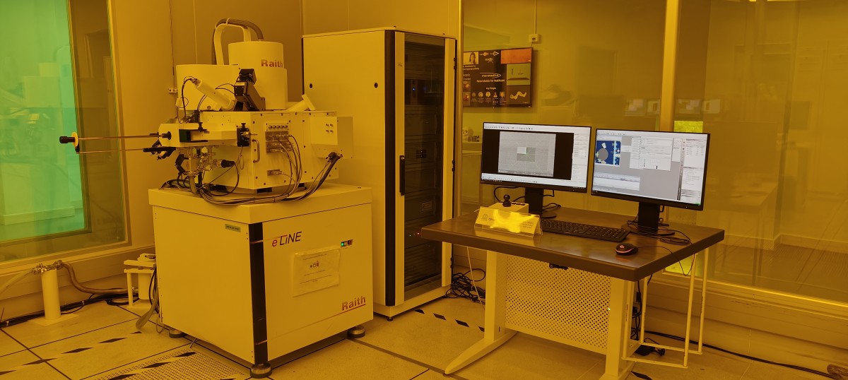
E-Beam Litho – Raith e-Line
Electron Beam Lithography (EBL) allows users to write patterns with extremely high resolution, smaller than 10nm in size. It makes use of a highly energetic, tightly focused electron beam, which is scanned over a sample coated with an electron-sensitive resist. The electron beam scans the image according to a pattern defined on a CAD file. The sample is then developed in an appropriate solvent which reveals the structures defined into the resist. This acts as a mold for subsequent pattern transfer techniques such as dry etching or metal lift-off. Due to the high-resolution nature of the technique, EBL has a vast range of applications including, but not limited to, nano-electronics, photonics, plasmonics, nano-fluidics, MEMS, x-ray and neutron optics.
NNfC has world class e-beam lithography facility with class 100 clean room and expertise in patterning of sub-20nm features.
This section will be updated soon.
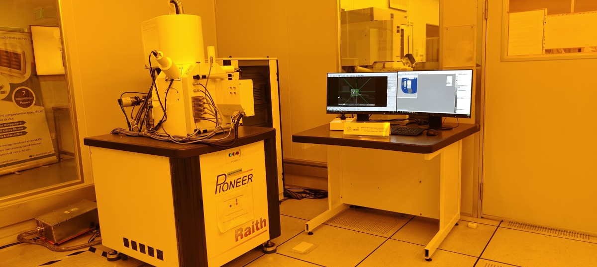
E-Beam Litho – Raith Pioneer
Electron Beam Lithography (EBL) allows users to write patterns with extremely high resolution, smaller than 10nm in size. It makes use of a highly energetic, tightly focused electron beam, which is scanned over a sample coated with an electron-sensitive resist. The electron beam scans the image according to a pattern defined on a CAD file. The sample is then developed in an appropriate solvent which reveals the structures defined into the resist. This acts as a mold for subsequent pattern transfer techniques such as dry etching or metal lift-off. Due to the high-resolution nature of the technique, EBL has a vast range of applications including, but not limited to, nano-electronics, photonics, plasmonics, nano-fluidics, MEMS, x-ray and neutron optics.
NNfC has world class e-beam lithography facility with class 100 clean room and expertise in patterning of sub-20nm features.
- Compact Electron Beam Lithography system with Thermal Field Emission technology
- Capable of sub 20nm lithography
- Maximum accelerating voltage 30kV and 7 apertures
- Morphology and Cross – section of various samples can be analysed
- Perfectly suited for write and view applications of samples with 2” area
This section will be updated soon.
Manual Wafer Bonder – EVG 501
EVG 501 Wafer Bonderhas the capability of Bonding 4″ wafers. The machine allows Anodic bonding, Eutectic bonding and Fusion bonding. Aligning wafer stack on EVG620 Mask aligner and anodically bonding the wafer stack on EVG bonder is also possible.
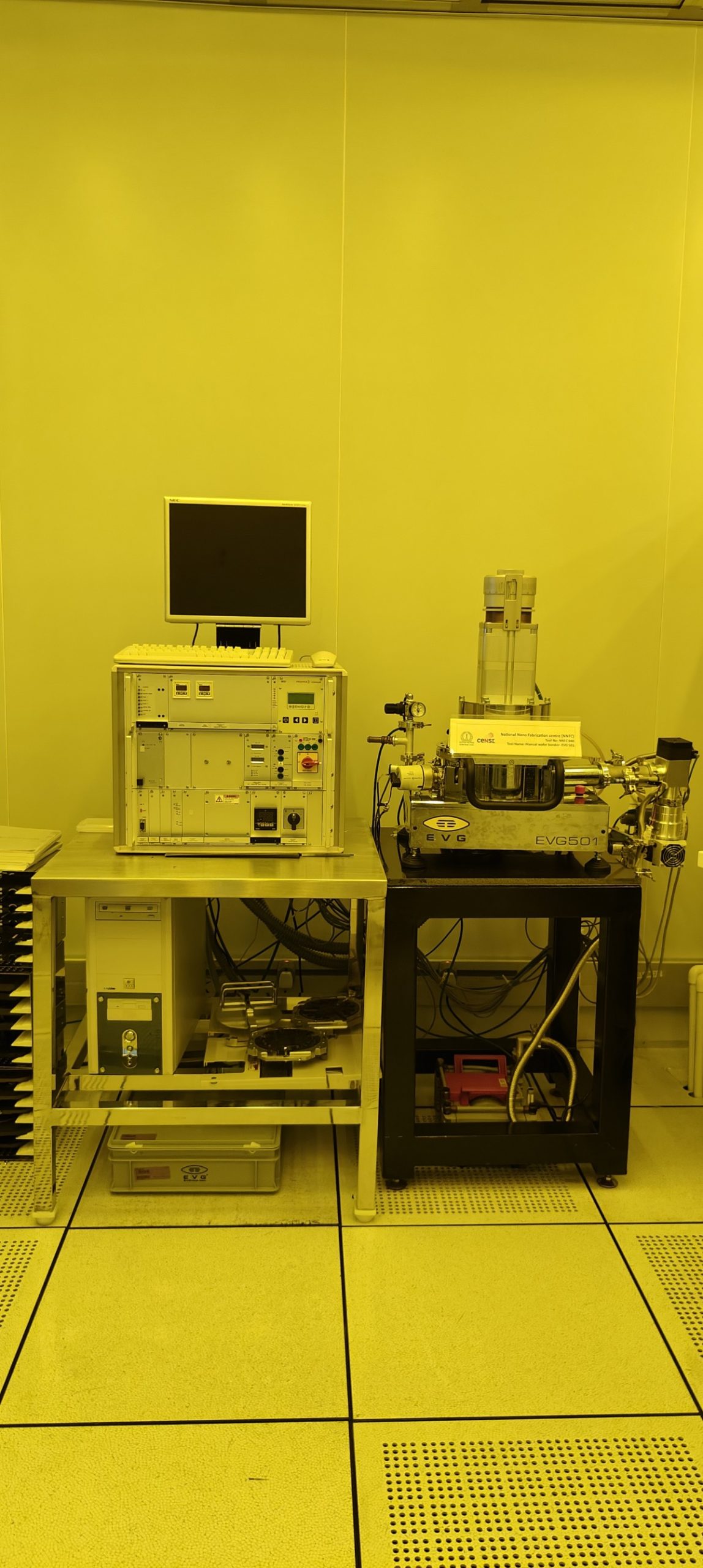
- Wafer/ Substrate Parameter : Up to 4 Inch Substrate and Quarter Wafer pieces can be handled
- Alignment Accuracy : 0.5µm for Glass/Silicon and 1µm for Silicon/Silicon
- Types of bonding Available: Eutectic bonding, Anodic bonding and Fusion bonding
- Adjustable from 0.5N – 40N
- Bond temperatures up to 450°C
- High-vacuum capable bond chamber (down to 10-5 mbar with turbo molecular pump)
- Temperature uniformity <+/- 1%
- Pressure uniformity <+/- 5%
This section will be updated soon.
Mask Aligner_EVG620NT
EVG620NT, the newest mask aligner to be added to NNFC’s optical Lithography bay incorparates NIL technology in addition to mask alignment
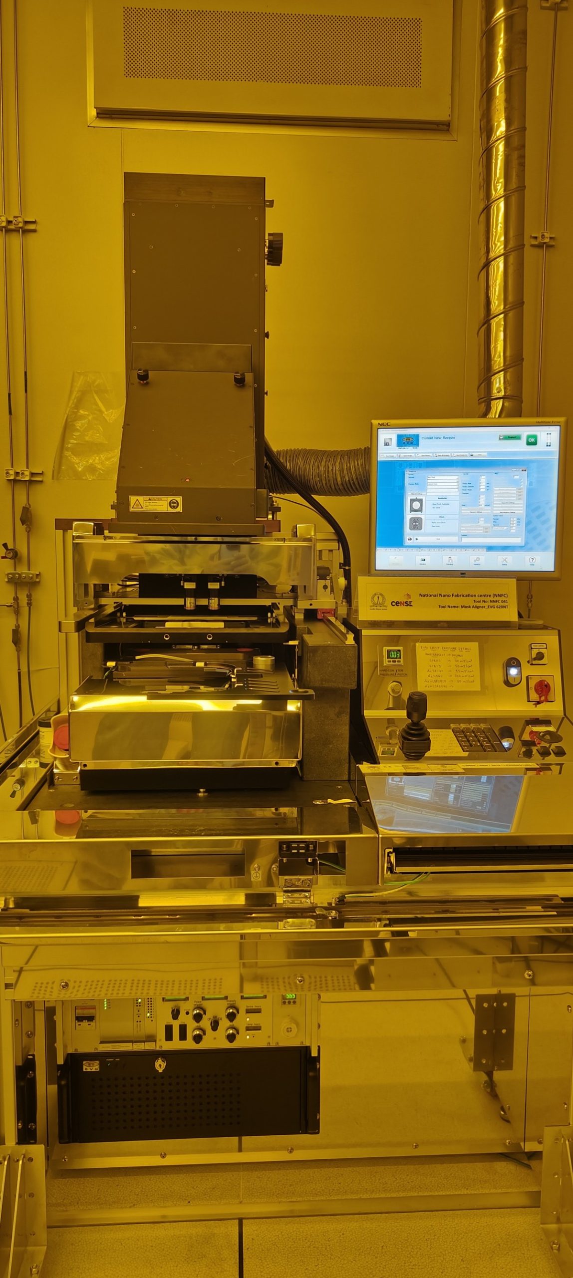

- Minimum feature size of 1um (lines/spaces with standard quartz mask)
- Auto alignment option for topside and backside
- Alignment accuracy – TSA (auto) <1um
BSA (auto) <1um
This section will be updated soon.
Mask Writer_Heidelberg DWL 66+
Heidelberg DWL66+ is a direct writing lithography tool which is capable of writing up to 9” substrate size. It is equipped with 405nm Diode Laser. The tool can resolve a minimum feature size of 600nm (Isolated Line) and 800nm of line with a pitch of 1.6µm. Front to Back Alignment and Grayscale exposure with 128 gray levels can be performed in the tool.
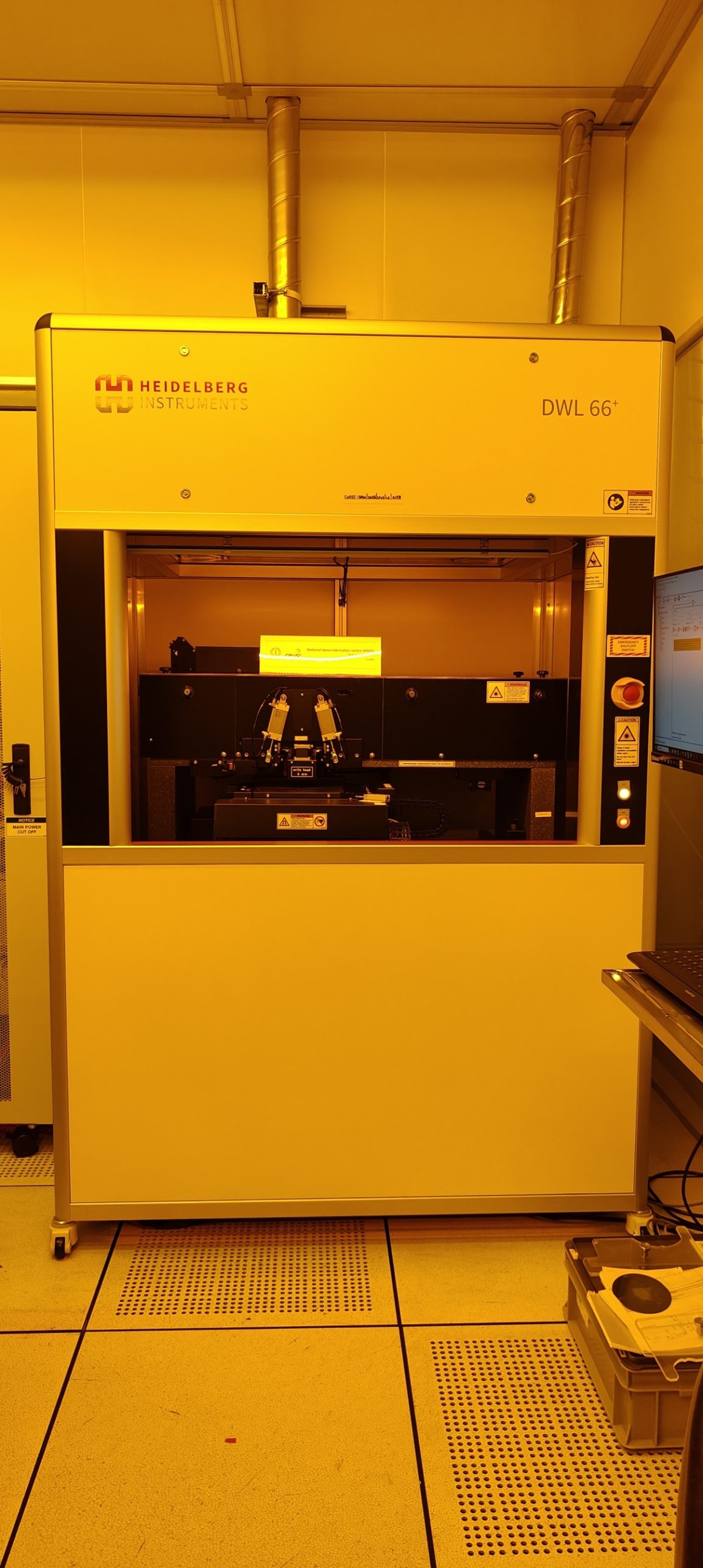
Exposure Wavelength – 405nm
Light Source – Diode Laser
Maximum Exposure Area – 200 x 200 𝑚𝑚2
Autofocus Mode – Pneumatic and Optical
Backside Alignment – Available
Autofocus Range – 80µm
Stich Width – 120µm
Grayscale – Available with 128 Gray Levels
Minimum Feature Size – 600nm (Isolated Line)
Minimum Line and Spacing – 800nm
This section will be updated soon.
Mask Writer_Heidelberg uMLA
Heidelberg µMLA is a direct writing lithography tool which is capable of writing up to 150 x 150 mm^2 area. It is equipped with 365nm LED. The tool can resolve a minimum feature size of 1µm (Isolated Line) and Line and Spacing of 1µm and 1.5µm respectively. Tool is capable of performing Grayscale exposure with 128 Gray Levels.
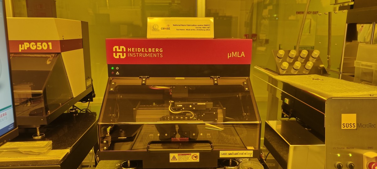
Exposure Wavelength – 365nm
Light Source – LED
Maximum Exposure Area – 150 x 150 𝑚𝑚2
Autofocus Mode – Pneumatic
Autofocus Range – 180µm
Grayscale – Available with 128 Gray Levels
Minimum Feature Size – 1µm (Isolated Line)
Minimum Line and Spacing – ≥ 1.5µm
This section will be updated soon.
Mask Writer_Heidelberg uPG501
An optolithography technique in which a laser beam/ LED is used to form the desired patterns on the photoresist is called laser /LED writing (Direct writing).
The specialty of the Mask Writer is that it can be used for direct pattern generation on any substrate using photolithographic principles with or without using a conventional mask plate. The main purpose of the Mask writer is to make photolithographic mask reticles and masks up to 5inch in Heidelberg µPG 501 system.
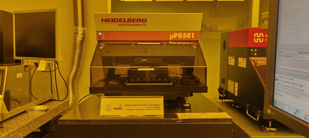
- Exposure wavelength – 390 nm
- Soda lime mask plate – Minimum line width of of 3 µm with gap of 3 µm of line width.
- Direct write for mask plates and wafers up to 5” × 5”
- Write speed up to 50 mm2/min
- GDS-2 and CIF Formats are preferable
- High Resolution Multi-Layer patterning capability using Alignment marks
- Primarily used for Mask Writing
- Direct writing on Substrate can also be done
This section will be updated soon.
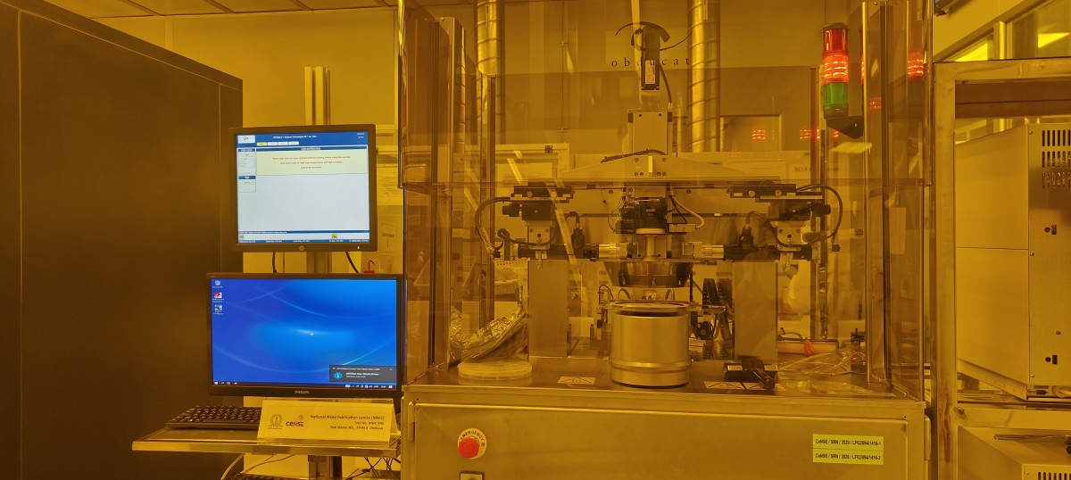
NIL_ EITRE 6 Obducat
Obducat EITRE 6 is a semiautomatic NIL tool allowing replications in micro and nano ranges.
| Specification | Minimum | Maximum |
| Substrate | 1 inch wafer | 6 inch wafer |
| Temperature (°c) | 20 | 200 |
| Pressure (bar) | 0 | 80 |
| UV source | 365 nm | |
| Heating System | 20°c/min | |
| Cooling system | 30°c/min | |
| Alignment accuracy | 1um (In pre optimized substrates) | |
- Capable of performing simultaneous thermal and UV NIL (STU) process
- Imprint of 70 nm pillars achieved with less than 15 nm of residual layer
- IPS usage increases the lifetime of master stamp (without contaminating the structures
This section will be updated soon.
Optical Lithography-MJB4
Suss MicroTec Mask aligner is a “SEMI-AUTOMATIC” Contact Photo-Lithographic Alignment and Exposure Tool with the above mentioned Specifications. It also has the Capability of Front to Back Alignment of Patterns. Recipes for different Exposure types and Contact Modes can be Pre-Written and is very User friendly.
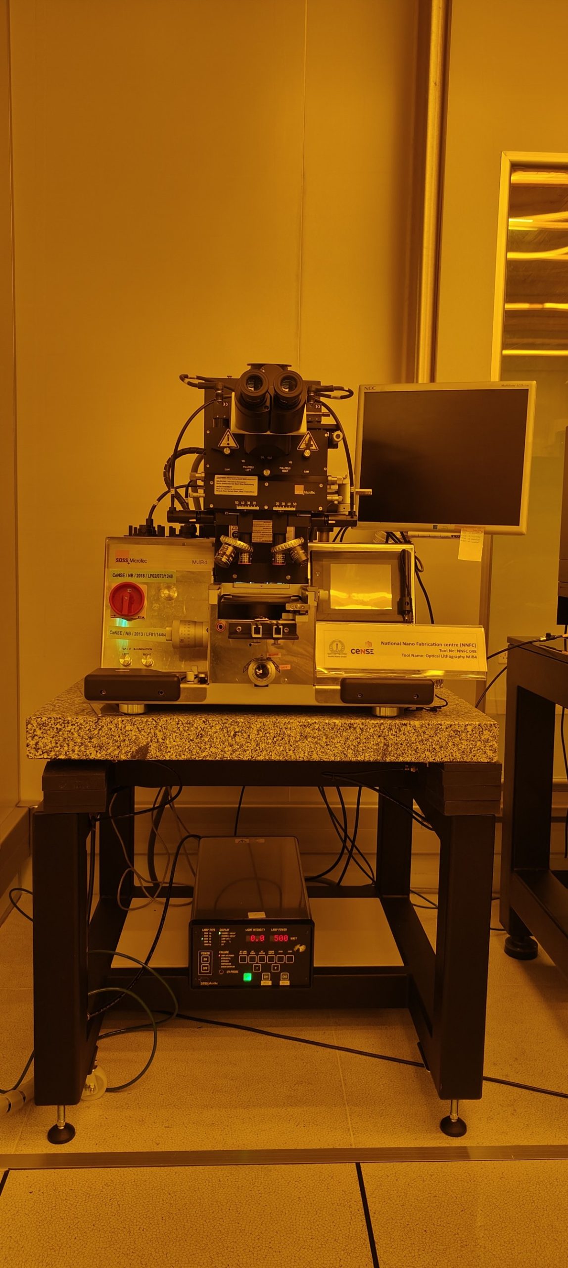
- Wafer/substrate parameter: 1” upto 4” * Mask parameter: Standard 2” x 2” to 5” to 5” (exposable are 1” upto 4”)
- Alignment accuracy: 0.5µm for top side and 5µm for bottom side
- Separation and proximity adjustment: 50 µm between mask and substrate
- Contact force between mask & substrate: 0.2 Bar to 2 Bar
- Contact modes: Soft, Hard, Low vacuum, Vacuum, Gap exposure
- Printing resolution: Less than 1µm in vacuum contact
This section will be updated soon.