KMOS Ultra Scan

Equipment Category: 

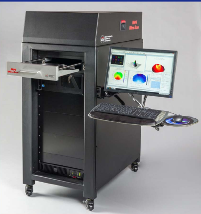
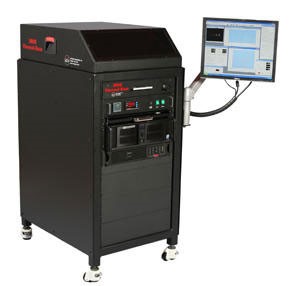
The Ultra-Scan uses a 2D laser array to map the two-dimensional curvature of semiconductor wafers, optical mirrors, lenses, or practically any polished surface. The system also provides quantitative film stress analysis with full area map scan for wafers by first scanning the bare substrate and then re-scanning the sample post-process.

  • Any polished surface with >1% reflectivity at laser λ
  • Spatial Scan Resolution: User selectable, down to 1um
  • Scanning is programmable.
  • 1cm/1cm sample can be measured.
  • Sample size range: 10mmx10mm – 200/300mm diameter
  • Bow, Curvature, Tilt etc can be done.
  • Various types of scan can be performed(Line, Circular, Rectangle, Custom line/Rectangle)
  • Laser Wavelength: 660nm nominal
You are not authorized to access this content.
Training is scheduled on every Monday
 
Timings: 10 AM to 12 PM.
 
Users must fill in the below Cleanroom Equipment Training Form for online training form in order to get trained 
 
You are not authorized to access this content.